Mimas-A7-Artix-7-Documentation
This site is a rewrite and improvement of the Mimas A7 Artix 7 Documentation, written as a collaboration effort with a lot of heavy lifting from @BlackIsDevin. You can view the original documentation here. The documentation listed is for the board’s Revision V3.0, though V2.0 does function similarly as well.
While the current state of the document is incomplete, this document eventually will serve as a viable replacement for the full documentation. As always, feel free to submit a pull request if you see any inconsistencies.
Board Power Limits
Unless otherwise specified, the board is capable of operating with a high
voltage ranging from 1.2V to 3.3V. Numato recommends to employ the LVCMOS33
I/O standard when connecting various parts. However, the LVCMOS18 standard
functions equivalently well with significantly less power draw..
Onboard 100MHz CMOS Oscillator
In original documentation, the onboard CMOS oscillator and its relevant connections have zero documentation past the specification that their operating square wave frequency is 100MHz, listed in the Technical Specifications section.
The clock output was determined (through various trial and error from
@BlackIsDevin) to be assigned to FPGA pin H4.
LED, Push Button and DIP Switch
The Mimas A7 comes equipped with four individual push buttons, as well as a pairing of eight binary-position DIP switches and eight indicator LEDs. The following is the connection image with the FPGA pin connections.

An important note that is not elaborated on in documentation is that the DIP switches, when flipped to the ON position (as marked on the FPGA) emit a logic LOW signal, as opposed to a logic HIGH. The same is true for the push buttons; When pushed down, they emit a logic LOW signal.
Assignments
On documentation, the LEDs and DIP switches are inverted from on the board, and LEDs are addressed from 1 instead of from 0 as listed on the board. The assignments are in the correct order; LD0 on board corresponds to D1 on documentation.
The push buttons are labelled BTNL, BTND, BTNR, and BTNU on board, but in documentation they are assigned numbers. For simplicity, the correct labels are annotated in blue.
7-Segment LED Display
As listed in original documentation, the 7-Segment LED display has the following pinout.
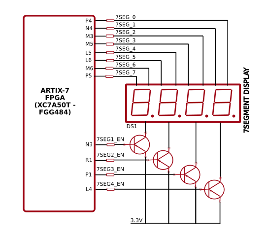
Each module can be separately turned on and off with the four enable lines
7SEGX_EN. Note that these are NOT write-enable lines - they are POWER-enable
lines. This means that, at any point in time if one enable line is not on, that
LED display will not be on.
While not listed in documentation, the data lines above correspond to the following segments (with data line numbers shown in green:)
The LED display data lines and enable lines are all active-LOW. This means to turn on the light for a specific segment, one must set the value to low.
The current limiting resistors for these diodes are 330R each.
Sample implementation
The following is some sample code demonstrating the active-LOW input nature of the seven segment LED display.
reg [3:0] sevenSegmentEnable;
reg [7:0] sevenSegmentData;

// The following code enables the second display from the left.
sevenSegmentEnable = 4'b1101;

// The following code writes the character '2'.
sevenSegmentData = 8'b01001100; // 2
In order to get the individual displays to display different numbers, one must utilize the clock input and switch each segment on/off constantly.
GPIOs
The Mimas A7 Artix 7 has several General Purpose Input/Output pins, that can be configured or reconfigured throughout I/O planning stages. The device is equipped with 80 user I/O pins that can be configured and wired (similar to breadboard headers) as through-hole connections.
All user I/O pin headers are length matched (the traces are equivalent in length, for timing purposes) and can be used as pairings in differential circuits as well.
P12 and P13 headers
The Mimas A7 features two 2x40 pin headers labeled P12 and P13, with each being located at the top and bottom of the card respectively. Each header features the following connections:
- 4 Vin pins
- 6 Vcc pins (connected to VCC_VADJ)
- 20 Ground pins
- 40 GPIO pins
- 10 Configuration pins
The exact GPIO and Configuration Pins that are connected to the P12 and P13 headers are detailed in the following image (blue is GPIO, purple is config):

An printable Excel spreadsheet featuring these pinout definitions can be found here. The spreadsheet is also sized so that the resulting print is the same scale as the pin headers (print 100% scale, don’t fit to page, double-sided).
Special thanks to @BlackIsDevin for compiling and coloring the charts above.